Read time 5 min
When a PCB antenna for Bluetooth device is the right choice?
Bluetooth2,4GHz ISM2.4 GHzPCB trace
When we design devices, our perspective differs from the end-user. We create a device piece by piece, where as the end-user sees the device as a whole. This also applies to evaluating the end product: the device either works or it doesn't. It doesn't matter if only one part fails, because with one malfunctioning part, the device can be a complete failure. A high-performing device requires proper integration of each part. After working on literally hundreds of antenna projects, we can safely say that we’ve encountered all kinds of integration problems along the way. Among those, one common issue is the improper use of an off-the-shelf antenna, such as a chip antenna.
This article emphasizes an essential point of product design: every tool, part and device has a proper way to use them– and deviating from that might have severe consequences. The same applies, whether we're talking about a laser cutter, a hammer or an antenna. Engineers are of course famously averse to reading instructions, but sometimes those instructions are there for a reason. Such is the case with off-the-shelf antennas, whose manufacturers provide reference design documents which should be followed to a T.
To illustrate our point, we are going to analyse how an off-the-shelf antenna component (SMD chip antenna) performs in a plastic surrounding, in which it was not originally designed to perform in. We then compare the results to a custom PCB trace antenna, designed by the engineers at Radientum. We will be using the antenna simulation method in this study, due to its cost-effectiveness and accuracy. If you want to know more about our methods, you can read our blog covering antenna simulations and simulation-driven approaches.
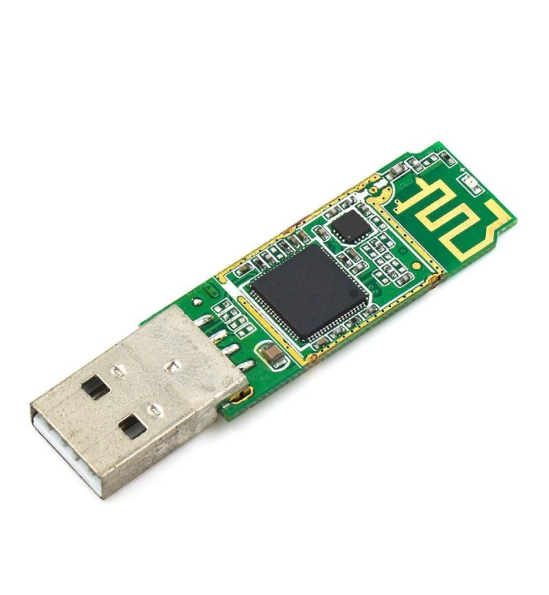
Let's start with the basics. Every wireless device needs an antenna, which can be either internal or external. Internal ones can be implemented using an SMD (Surface Mounted Device) chip antenna component, or it can be designed on a PCB (Printed Circuit Board). Internal antennas can also integrate with the device’s mechanics. For any off-the-shelf antennas, the antenna component manufacturer provides a test board indicating the environment where the antenna is designed to work.
To choose a common form factor for our sample device, we decide on one that is a characteristic among most IoT and many wearable devices: a plastic cover. For the sake of presentation, let’s take this one step further, and make the device so compact that the plastic cover is actually touching the antenna. Size of the PCB and antenna GND clearance follow the test board of antenna component manufacturer.

The first parameter to look at is Return Loss or VSWR. We have discussed different methods to measure this parameter in our earlier blog concerning measurements. In Picture 2 below, we present a few interesting results:

Let’s introduce another measure to get a more in-depth look at what happened. Picture 3 below shows total antenna efficiency. The introduction of the plastic surrounding transformed a good chip antenna with -2dB efficiency into an antenna that has lowest efficiency of -15dB at the highest frequency. The peak performance remains tolerable (the blue curve), but tuning shifted to a new frequency band, which is far from the original design.

So, how can we fix this? Fortunately antenna manufacturers provide instructions on how to change the matching components in their technical datasheet or reference design board. In this demonstration, we will try two ways to do that. First, we retain the same component topology, but alter the component values. Later we will devise a new component topology. We are able to accomplish both relatively quickly with our modern simulation tools. If we had to use traditional prototypes, this might require several trials.
The pink curve “S1,1 ChipAnt Plastic RefComp Tuning” in the first graph (Picture 2) shows what can be accomplished with the first approach. We achieve a notable improvement of 1,5 dB in matching level at 700MHz, but no improvement at 960MHz. The red curve in Picture 3, which depicts the efficiency of this approach, shows clear improvement with most of the frequency band. However, the highest frequencies remain unchanged. Minimum efficiency level across the band is still around -15dB.
Next, we'll explore a new matching component topology, which was designed to optimize the entire frequency band – including the highest frequencies. This is shown by the red matching curve in Picture 2, and the pink efficiency curve in Picture 3 “ChipAnt NewComp Opt”. The matching level is quite flat at -2dB, but demonstrates an improvement of 1dB at 960MHz. This matching level leads to around 1dB worse efficiency at 700MHz, but a clear improvement above 800MHz and more than 1dB at 960MHz. This means that the worst efficiency level over the 700-960MHz is now about -14dB, instead of -15dB. Doesn’t this improvement sound quite small? You are absolutely right, it does. Let’s find a solution, while figuring out why we weren't able to improve it more.
The real, underlying reason behind the poor performance was more fundamental than wrong matching. Due to the added plastic surrounding, the component itself was no longer functional. When encountering such problems in product development, there are two options on how to move forward: either you alter the product form factor, or you customize the antenna. Here we focus on the latter option.
Unless you are ordering a custom antenna component from an antenna manufacturer, usually the easiest solution is to restart from scratch. While it requires extra work due to its custom design, a PCB trace antenna can be designed for the same space as a chip antenna.

Let's look at Picture 5 to see how we performed. The difference is as clear as night and day! The PCB trace antenna (green curve) that has been designed for the plastic environment vastly outperforms the chip antenna reference component topology (red curve). Efficiency is up to 20 times better at 960MHz! In fact, this performance level matches the ideal test board situation for the chip antenna without plastics. This right here shows what professionals are able to design.

There’s a few things to take a note of. First of all, it is important to keep in mind that the antenna performance is dependent on its surroundings. A good antenna in free space might not perform at the same level in your practical application. Fine-tuning and matching are also always necessary. And finally, one of the easiest and most cost-effective ways to ensure your product’s wireless performance is to test the performance with simulation tools.
Radientum can help you to integrate antenna components from selected vendors using our simulations into your specific product. We can also develop custom solutions to PCB, FPC, LDS, etc. Read more about our services from here.