Read time 10 min
Understanding Antenna Gain: Insights for Great Wireless Performance
Antenna TestingAntennaGain
For Bluetooth device designers, choosing a Bluetooth printed circuit board (PCB) trace antenna, also referred to as a PCB trace antenna, microstrip antenna, or just as PCB antenna, is rarely straightforward. In theory, it is highly attractive: no bill of materials (BOM) cost for the antenna itself, no connectors, and no external RF components.
But in real products, antenna performance is defined by integration, not by the antenna geometry alone.
In this article, we break down when a PCB antenna for Bluetooth is the right choice, when it becomes a risk, and what hardware teams should evaluate early, especially for industrial and B2B products where reliability, range, and predictability matter more than up front cost.
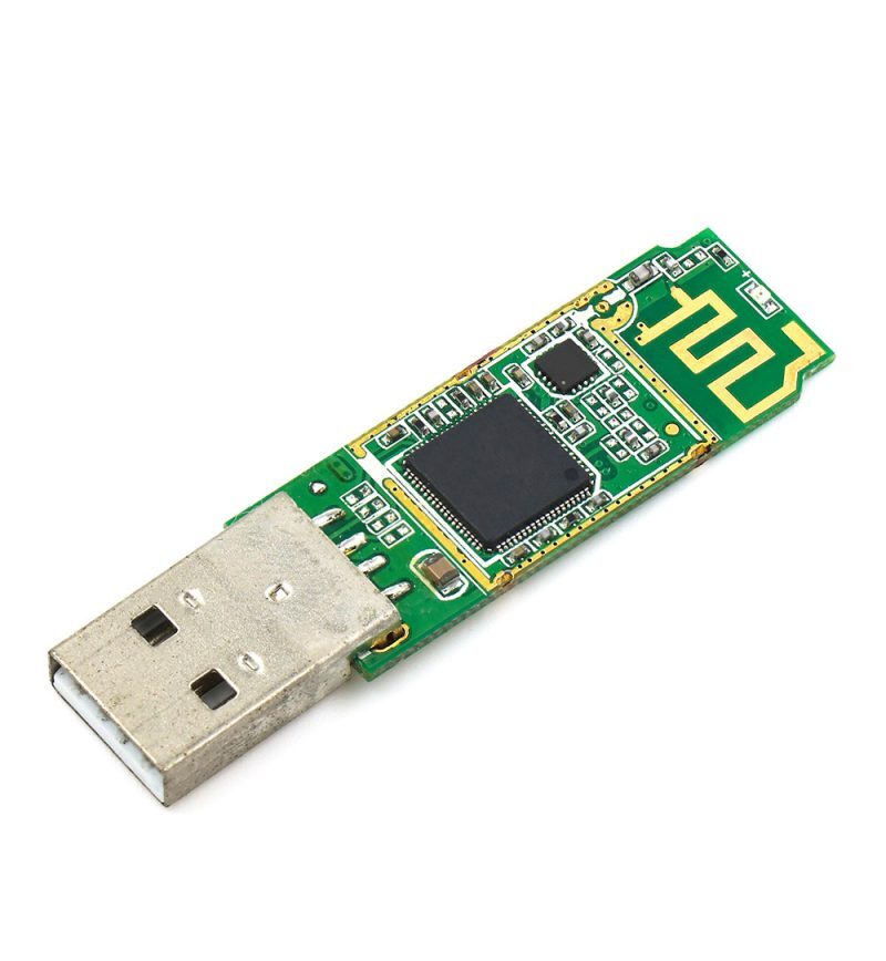
A PCB trace antenna is an antenna formed directly from copper on the PCB, typically as an inverted‑F antenna (IFA), meandered monopole, or loop structure. Unlike chip or external antennas, the PCB itself is the only radiating structure.
Common terms you’ll see used interchangeably include:
From a manufacturing perspective, the appeal is obvious: zero component cost and full control over geometry.
From an RF perspective, it comes with strict constraints.
A PCB antenna can be an excellent solution when the following conditions are met.
PCB antennas are highly sensitive to their environment. They work best when:
This is often the case in industrial sensors, gateways, and fixed installations, where the form factor doesn’t change between revisions.
If the mechanical design is still evolving, a PCB antenna has to evolve with it.
For many Bluetooth Low Energy (BLE) devices, the goal isn’t maximum range. It’s consistent and predictable coverage.
PCB trace antennas are well suited when:
For professional products, repeatability is often more important than peak performance. For peak performance there are other options available such as flex or LDS.
A PCB antenna is not a drop‑in element. Its performance depends on:
If your team controls the full PCB layout, and can reserve sufficient keep‑out area, a printed Bluetooth antenna can be tuned very precisely. This is where PCB antennas outperform many commercial off-the-shelf (COTS) alternatives.
Because there are no connectors, springs, or cables, on‑board antennas offer:
For industrial and B2B products shipped over many years, this can be a decisive advantage.
Just as important is knowing when not to use a Bluetooth PCB trace antenna.
In small devices with batteries, displays, or metal housings, PCB antennas don't have the space once the final mechanics are added.
What looks good on a bare PCB can fail badly in the real product.
This is a common root cause of late‑stage Bluetooth performance issues.
For standard Bluetooth communication, metrics like efficiency and gain are often enough.
But for advanced use cases, such as Bluetooth Channel Sounding, antenna behavior across frequency and angle becomes critical.
Channel Sounding performance depends heavily on antenna group delay stability, not just matching or efficiency. Many PCB antennas or COTS antennas that work “fine” for communication are not suitable once precise ranging is required.
A PCB antenna is not portable between products. Even small layout, stackup or enclosure changes can invalidate previous tuning.
If your roadmap includes multiple form factors or variants, a custom PCB antenna may increase long‑term engineering effort unless managed carefully from the start.
With Bluetooth 6.0 introducing Channel Sounding, antenna design moves from being “good enough” to being fundamental system performance.
Accurate ranging requires:
The Bluetooth Channel Sounding whitepaper shows that bluetooth antennas performing well on bare PCBs can fail completely once integrated into real devices—and that redesigning the antenna specifically for the final product is often required.
This is where early antenna decisions have huge impact.
A Bluetooth PCB trace antenna is the right choice when:
It becomes risky when:
In other words: Bluetooth PCB antennas reward early, system‑level thinking—and punish late fixes.
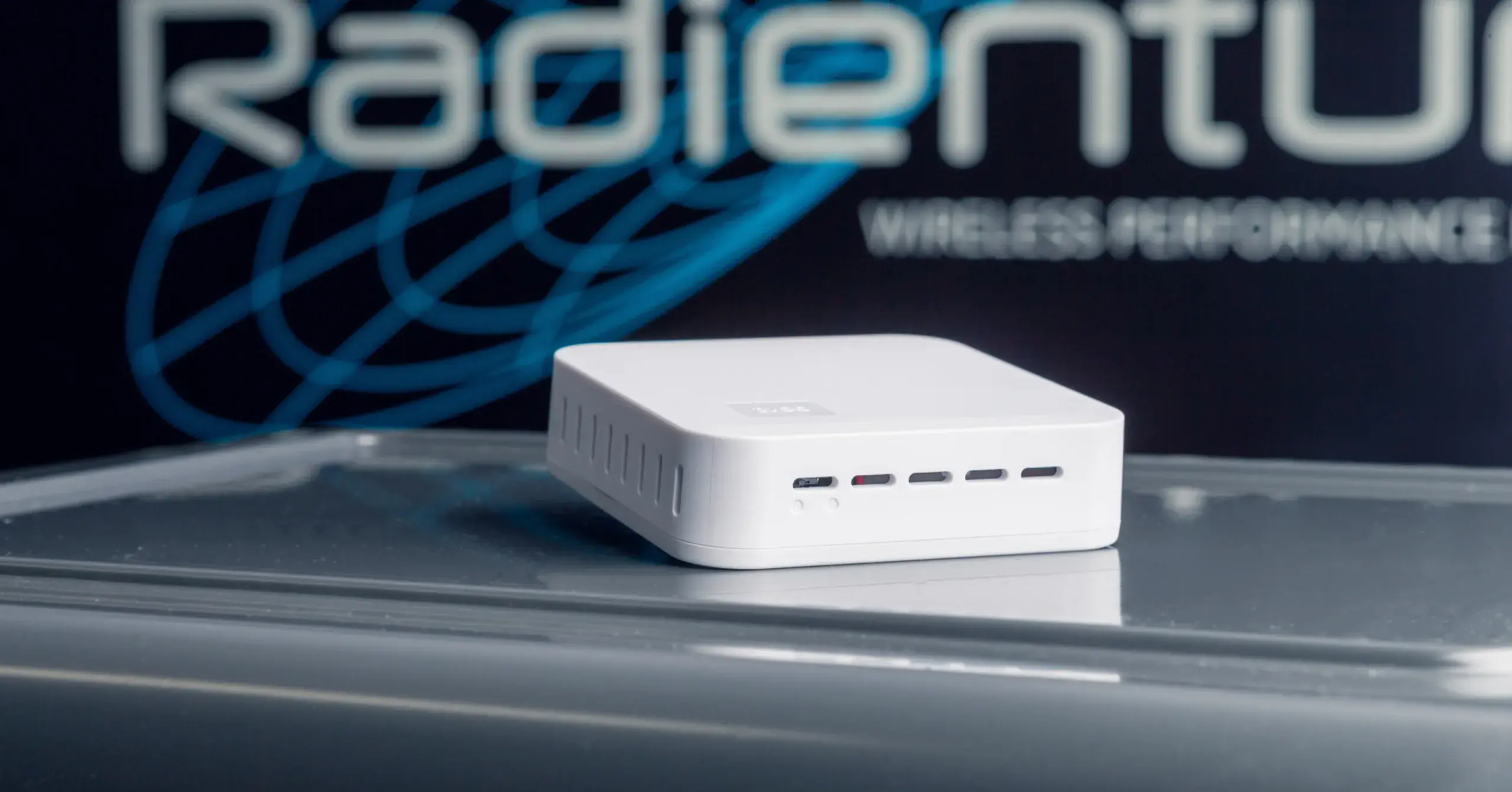
Radientum helps hardware teams choose, design, and validate the right antenna architecture, from PCB antennas to multi‑antenna systems, based on the actual product environment.
We support companies with:
Learn more about Radientum’s antenna design services and how we de‑risk wireless performance early in product development.